As a PCBA (Printed Circuit Board Assembly) supplier, I understand the paramount importance of inspection in ensuring the quality and reliability of our products. In this blog, I’ll delve into the various inspection methods for PCBA that we employ to meet strict industry standards and exceed our customers’ expectations. PCBA
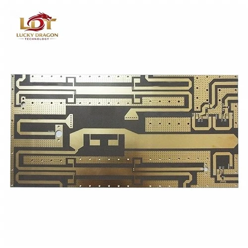
Visual Inspection
Visual inspection is the most fundamental and straightforward method in PCBA inspection. It involves using the naked eye or magnification tools such as microscopes to examine the assembled PCB for obvious defects. This method is typically the first step in the inspection process and is crucial for identifying issues at an early stage.
When conducting a visual inspection, we look for several key aspects. Firstly, we check for the correct placement of components. This includes verifying that each component is positioned in the right location on the PCB, with proper orientation. For example, SMD (Surface-Mount Device) components need to be precisely aligned to their designated pads, and through-hole components should be inserted correctly into their respective holes.
Secondly, we inspect the soldering joints. A good soldering joint should have a smooth, shiny appearance and be free of cracks, voids, or bridges. Cracks in the soldering joints can lead to intermittent electrical connections, while bridges between adjacent pads can cause short – circuits. Voids in the solder can reduce the mechanical strength and electrical conductivity of the joint.
We also look for any signs of physical damage to the components or the PCB itself. This could include broken leads on components, scratches on the PCB surface, or delamination of the PCB layers. Visual inspection can be time – consuming, especially for complex PCBs with a large number of components, but it is an essential part of our quality control process.
Automated Optical Inspection (AOI)
Automated Optical Inspection (AOI) is a highly efficient and accurate inspection method that uses high – resolution cameras and advanced image – processing algorithms to detect defects on PCBA. AOI systems can quickly scan the entire PCB surface, capturing detailed images of components and soldering joints.
One of the main advantages of AOI is its speed. It can inspect a PCB in a matter of seconds, making it suitable for high – volume production environments. AOI systems can detect a wide range of defects, including component missing, misaligned components, incorrect polarity, and soldering defects such as solder bridges and insufficient solder.
The image – processing algorithms in AOI systems are programmed to compare the captured images with a pre – defined reference image. Any deviations from the reference image are flagged as potential defects. For example, if a component is missing, the AOI system will detect the empty pad and mark it for further inspection.
However, AOI also has its limitations. It may not be able to detect some internal defects, such as cracks inside the components or hidden soldering issues. Additionally, AOI systems need to be properly calibrated to ensure accurate results. False positives can occur if the lighting conditions or the reference image is not set correctly.
X – Ray Inspection
X – ray inspection is a powerful method for detecting internal defects in PCBA that are not visible through visual or AOI inspection. This method uses X – rays to penetrate the PCB and components, allowing us to see the internal structure.
X – ray inspection is particularly useful for detecting hidden soldering defects, such as voids in BGA (Ball Grid Array) packages. BGA components have a large number of solder balls underneath them, and it is difficult to inspect these solder joints using traditional methods. X – ray inspection can clearly show the condition of these solder balls, including any voids or misalignments.
Another application of X – ray inspection is in detecting the correct placement of components with internal structures, such as multi – layer capacitors. X – rays can reveal if the internal layers of these components are intact and correctly aligned.
There are two main types of X – ray inspection systems: 2D and 3D. 2D X – ray systems provide a flat, two – dimensional view of the PCB, which is suitable for detecting basic internal defects. 3D X – ray systems, on the other hand, can provide a more detailed, three – dimensional view of the PCB, allowing for more accurate defect detection. However, 3D X – ray systems are more expensive and require more advanced training to operate.
In – Circuit Testing (ICT)
In – Circuit Testing (ICT) is a comprehensive electrical testing method that checks the functionality of individual components and the electrical connectivity of the PCB. ICT systems use a bed – of – nails fixture that makes electrical contact with specific test points on the PCB.
During ICT, the system applies a series of electrical signals to the PCB and measures the responses. By comparing the measured responses with the expected values, the system can determine if there are any faults in the components or the electrical connections. For example, ICT can detect open circuits, short circuits, and incorrect component values.
One of the advantages of ICT is its high accuracy. It can precisely identify the location of a fault, which is very helpful for debugging and rework. ICT is also suitable for testing a wide range of components, including resistors, capacitors, diodes, and integrated circuits.
However, ICT also has some drawbacks. The cost of developing a bespoke bed – of – nails fixture can be quite high, especially for complex PCBs. In addition, ICT may not be able to test some components that require specific operating conditions or software to function properly.
Functional Testing
Functional testing is the final and most important step in PCBA inspection. This method tests the overall functionality of the assembled PCB in a real – world or simulated environment. The goal of functional testing is to ensure that the PCBA can perform its intended functions as expected.
Functional testing can be customized according to the specific requirements of the product. For example, for a mobile phone PCB, functional testing may include testing the touchscreen, camera, audio output, and wireless connectivity. The testing equipment and procedures are designed to mimic the actual usage scenarios of the product.
Functional testing can detect a wide range of issues that may not be discovered through other inspection methods. It can identify problems related to software – hardware integration, system – level performance, and environmental factors. However, functional testing can be time – consuming and expensive, especially for complex products.
Conclusion

In conclusion, a combination of these inspection methods is essential for ensuring the high quality and reliability of PCBA. At our company, we use a multi – stage inspection process that starts with visual inspection and progresses through AOI, X – ray inspection, ICT, and functional testing. This comprehensive approach allows us to detect and correct any defects at different stages of the production process, minimizing the risk of faulty products reaching our customers.
PCB If you are in the market for high – quality PCBA, we are here to provide you with reliable products and excellent service. Our team of experts is dedicated to meeting your specific requirements and ensuring your satisfaction. Please feel free to contact us for a quote or to discuss your procurement needs.
References
- “Handbook of Printed Circuit Board Design, Fabrication, and Assembly” by Clyde F. Coombs Jr.
- “Electronics Manufacturing Technology Handbook” edited by Tom Ippolito.
- “Automated Optical Inspection for Printed Circuit Boards” by various industry research papers.
Lucky Dragon Technology Shenzhen Co., Ltd.
With abundant experience, we are one of the most professional PCBA manufacturers and suppliers in China. We warmly welcome you to buy bulk high quality PCBA for sale here from our factory. If you have any enquiry about cooperation, please feel free to email us.
Address: 5th Floor, Building 1, Jinshan Industrial Park, 375, Xixiang Section, Guangshen Road, Xixiang Street, Baoan District, Shenzhen City, Guangdong Province, China
E-mail: sales@Ldtac.com
WebSite: https://www.ldtac.com/
